(China (Mainland))


Product Summary
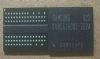
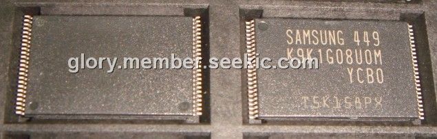
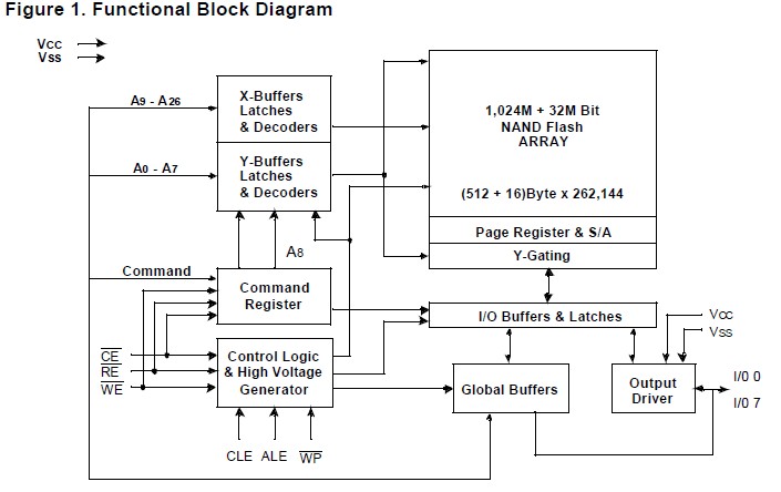
The K9K1G08U0M-YCB0 is a 128M(134,217,728)x8bit NAND Flash Memory with a spare 4.096K(4,194,304)x8bit. Its NAND cell provides the most cost-effective solution for the solid state mass storage market. A program operation of the K9K1G08U0M-YCB0 can be performed in typical 200ms on the 528-byte page and an erase operation can be performed in typical 2ms on a 16K-byte block. Data in the page can be read out at 50ns cycle time per byte. The I/O pins of the K9K1G08U0M-YCB0 serve as the ports for address and data input/output as well as command inputs. The on-chip write controller automates all program and erase functions including pulse repetition, where required, and internal verification and margining of data. Even the write-intensive systems can take advantage of the K9K1G08U0M-YCB0 extended reliability of 100K program/erase cycles by providing ECC(Error Correcting Code) with real time mapping-out algorithm. The K9K1G08U0M-YCB0 is an optimum solution for large nonvolatile storage applications such as solid state file storage and other portable applications requiring non-volatility.
Parametrics
K9K1G08U0M-YCB0 absolute maximum ratings: (1)Voltage on any pin relative to VSS: VIN: -0.6 to + 4.6 V; VCC: -0.6 to + 4.6 v; (2)Temperature Under Bias, TBIAS: -10 to +125℃; (3)Storage Temperature, TSTG: -65 to +150 ℃.
Features
K9K1G08U0M-YCB0 features: (1)Voltage Supply : 2.7V~3.6V; (2)Organization: Memory Cell Array : (128M + 4,096K)bit x 8bit; Data Register: (512 + 16)bit x8bit multipled by eight planes; (3)Automatic Program and Erase: Page Program : (512 + 16)Byte; Block Erase : (16K + 512)Byte; (4)528-Byte Page Read Operation: Random Access : 12us(Max.); Serial Page Access : 50ns(Min.); (5)Fast Write Cycle Time: Program time : 200us(Typ.); Block Erase Time: 2ms(Typ.); (6)Command/Address/Data Multiplexed I/O Port; (7)Hardware Data Protection: Program/Erase Lockout During Power Transitions; ; (8)Reliable CMOS Floating-Gate Technology: Endurance: 100K Program/Erase Cycles; Data Retention : 10 Years; (9)Command Register Operation; (10)Intelligent Copy-Back Operation; (11)Package: 48 - Pin TSOP I (12 x 20 / 0.5 mm pitch); (12)Simultaneous Four Page/Block Program/Erase.
Diagrams
| Image | Part No | Mfg | Description |  |
Pricing (USD) |
Quantity | ||||
|---|---|---|---|---|---|---|---|---|---|---|
 |
 K9K1G08U0M-YCB0 |
Other |
|
Data Sheet |
Negotiable |
|
||||
| Image | Part No | Mfg | Description | |
Pricing (USD) |
Quantity | ||||
|
K9K1208D0C |
Other |
|
Data Sheet |
Negotiable |
|
||||
|
K9K1208Q0C |
Other |
|
Data Sheet |
Negotiable |
|
||||
|
K9K1208Q0C-XXB0 |
Other |
|
Data Sheet |
Negotiable |
|
||||
|
K9K1208U0A-YCB0 |
Other |
|
Data Sheet |
Negotiable |
|
||||
|
K9K1208U0A-YIB0 |
Other |
|
Data Sheet |
Negotiable |
|
||||
|
K9K1208U0C |
Other |
|
Data Sheet |
Negotiable |
|
||||